Protecting highly sensitive internal optical systems and electronic sensors from harsh external environments without degrading signal integrity or beam quality is a fundamental engineering challenge. When designing advanced optical instruments, engineers must isolate delicate internal components from vacuum, high pressure, extreme temperatures, and abrasive particulates. Failing to establish this barrier compromises the entire system.
The cost of improper specification is severe. Using the wrong material or inadequate surface tolerance for an Optical Window leads to beam distortion, thermal lensing, sensor failure, or catastrophic equipment damage in pressurized environments. A component that seems simple on the surface dictates the success or failure of complex laser or imaging systems.
This article provides a technical evaluation framework for engineers and procurement teams. You will learn how to specify the correct component based on transmission requirements, environmental stressors, and operational constraints, ensuring reliable performance across demanding industrial applications.
Key Takeaways
- Zero Optical Power: An optical window is designed to separate environments without altering magnification or focal length, requiring strict parallelism and flatness.
- Beyond Protection: While primarily deployed for optical protection, specialized optical windows also serve auxiliary roles like beam sampling (reflecting a small fraction of light) and phase/optical path compensation.
- Material Dictates Capability: The choice between materials like Fused Silica, Sapphire, and N-BK7 determines the transmission spectrum (UV, VIS, IR) and thermal/mechanical survivability.
- Surface Quality Impacts Performance: High-power laser and imaging applications require stringent scratch-dig specifications to prevent scatter and localized heating.
- Mounting is Critical: Even the highest-quality optical window will fail or distort if mechanical mounting introduces stress-induced birefringence or compromises the pressure seal.
What is an Optical Window?
Core Functionality
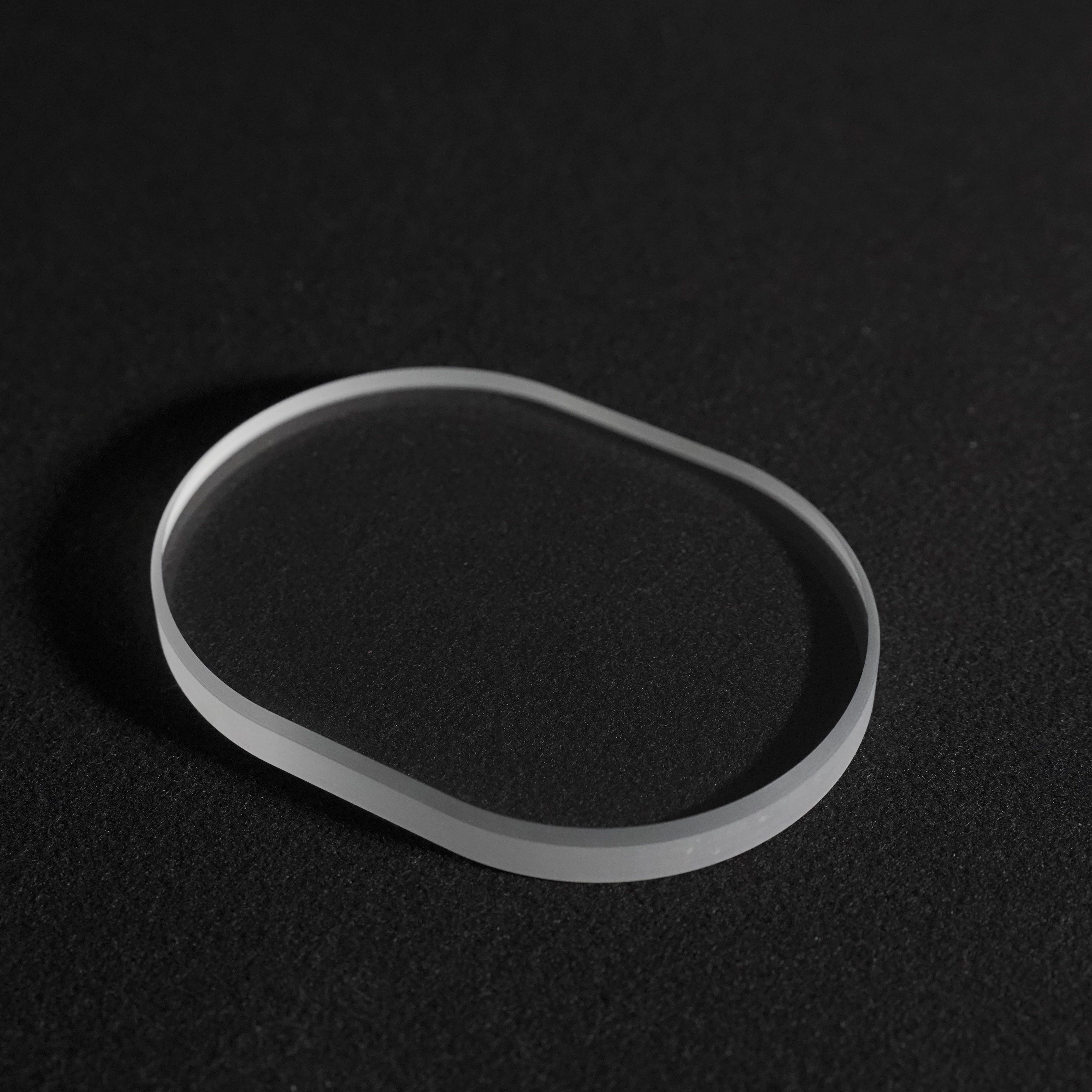
At its core, this component is a flat, parallel, optically transparent barrier. Its primary purpose is environmental separation. It isolates internal components from vacuums, high pressures, moisture, and flying particulates. It achieves this isolation without introducing optical power into the system. Light passes through the barrier without experiencing changes in focal length or magnification, preserving the original optical path. Engineers rely on this neutrality to maintain system calibration. Any deviation in the substrate introduces errors that compound throughout the optical train.
Optical Window vs. Standard Protective Glass
Precision optical components differ vastly from commercial protective glass. Standard glass lacks the strict manufacturing controls required for advanced optics. Precision windows feature tightly controlled transmitted wavefront error (TWE) and parallelism. Substrate purity is meticulously managed to ensure a consistent refractive index across the entire aperture. This prevents the image distortion and beam deviation common with lower-grade materials. When you specify a precision component, you are paying for the absence of optical interference.
| Specification | Standard Glass | Precision Optical Window |
| Surface Flatness | > 2 waves | λ/4 to λ/20 |
| Parallelism | > 3 arcminutes | < 10 arcseconds |
| Scratch-Dig | 80-50 or worse | 40-20 to 10-5 |
| Material Purity | Commercial grade (bubbles/inclusions common) | Optical grade (striae-free, high homogeneity) |
The Role of Optical Protection
These components act as sacrificial or shielding layers for high-value internal hardware. Lenses, sensitive detectors, and laser diodes are highly susceptible to environmental degradation. By implementing robust optical protection, engineers ensure that abrasive dust, chemical splashes, or extreme heat damage only the easily replaceable external barrier. This strategy protects the critical internal architecture. Replacing a front-element barrier takes minutes and costs a fraction of replacing a complex objective lens or a damaged sensor array.
Secondary Optical Roles
Beyond simple shielding, windows perform secondary optical functions. They facilitate beam sampling by reflecting a small, predictable percentage of a beam via Fresnel reflection. This allows operators to monitor power levels without interrupting the main beam path. They also act as compensator plates to balance optical path length (OPD) and dispersion in interferometers and complex multi-component setups. In these applications, the exact thickness and refractive index of the substrate are calculated to offset phase shifts introduced elsewhere in the system.
Primary Industrial Applications and Use Cases
Laser Processing and Manufacturing
Industrial cutting, welding, and marking systems rely heavily on a specialized laser window. These applications demand high damage thresholds and low absorption rates. If the material absorbs even a fraction of the high-power laser energy, localized heating occurs. This thermal lensing alters the refractive index, distorting the beam profile and ruining the precision of the manufacturing process. For multi-kilowatt fiber lasers, the substrate must exhibit near-zero bulk absorption. Contamination on the surface can trigger catastrophic failure, making proper specification and maintenance mandatory.
Machine Vision and Automated Inspection
Factory floors present hostile environments for sensitive camera sensors. Dust, cutting oils, and metallic debris threaten automated quality control systems. Optical barriers protect these sensors while maintaining the high contrast and resolution necessary for machine vision algorithms to detect micro-defects accurately. In high-speed sorting applications, any optical distortion from a low-quality barrier can cause false rejects or missed defects. The barrier must transmit the specific wavelengths used by the inspection lighting, whether that is visible white light or specific infrared bands.
Industrial Equipment Monitoring
Visual inspection viewports are necessary for monitoring hazardous processes. High-temperature furnaces, chemical reaction chambers, and pressurized tanks require safe viewing access. Operators and remote cameras depend on highly durable, transparent barriers to monitor internal conditions without risking exposure to toxic chemicals or explosive pressures. These viewports often utilize materials like Sapphire or specialized quartz to withstand continuous exposure to extreme heat and corrosive gases without clouding or degrading over time.
Aerospace and Defense Sensors
Airborne and terrestrial targeting systems operate under extreme conditions. Sensors face rapid temperature fluctuations, high-altitude pressure changes, and abrasive airborne particulates like sand. The optical barriers deployed in these systems must survive these mechanical and thermal shocks while maintaining absolute optical clarity for targeting and imaging. They are often subjected to rigorous MIL-SPEC testing for salt fog, humidity, and severe abrasion. The coatings applied to these substrates must be exceptionally hard to prevent delamination during flight.
Vacuum and Pressure Chambers
In viewport applications, the window serves a structural role. It must withstand significant pressure differentials between the internal chamber and the external atmosphere. Engineers calculate the exact thickness required to prevent mechanical failure or catastrophic implosion. They balance structural integrity with optical transmission. A substrate that is too thin will bow under pressure, introducing optical distortion before it shatters. A substrate that is too thick will unnecessarily attenuate the transmitted signal and increase the overall weight of the assembly.
Material Selection: The Foundation of Optical Performance
N-BK7 and Borosilicate
N-BK7 and Borosilicate are standard materials for cost-effective applications operating in the visible and near-infrared (NIR) spectrums. They offer excellent transmission and are relatively easy to manufacture. They are best suited for environments where extreme thermal shock and high-power laser damage are not primary concerns. N-BK7 is the default choice for high-quality visible imaging applications due to its high homogeneity and low bubble content. Borosilicate offers slightly better thermal resistance, making it suitable for moderate-temperature viewports.
UV Fused Silica
UV Fused Silica provides significant advantages for demanding applications. It offers exceptional deep UV transmission and features a very low coefficient of thermal expansion (CTE). This low CTE makes it highly resistant to thermal shock. Its high resistance to laser damage makes it the preferred choice for high-power laser systems. Unlike standard glass, UV Fused Silica does not fluoresce under intense UV illumination, which is critical for fluorescence microscopy and semiconductor inspection equipment.
Sapphire
Sapphire dominates in high-pressure, highly abrasive environments. It possesses extreme hardness, second only to diamond among standard optical materials. Sapphire offers a broad transmission range from UV to mid-infrared and features high thermal conductivity, allowing it to dissipate heat rapidly in harsh industrial settings. Its crystalline structure makes it highly resistant to chemical attack from strong acids and alkalis. However, its birefringence requires careful axis orientation during manufacturing to prevent polarization issues in sensitive optical systems.
Infrared (IR) Materials
Thermal imaging and CO2 laser applications require specialized IR materials like Zinc Selenide (ZnSe), Germanium (Ge), and Silicon (Si). These materials transmit wavelengths that standard glass absorbs. Engineers must account for specific handling requirements. Some IR materials, like ZnSe, are toxic and require strict safety protocols during handling and disposal. Germanium offers excellent transmission in the 8-12 micron range but becomes opaque at elevated temperatures, limiting its use in high-heat environments without active cooling.
| Material | Transmission Range | Index of Refraction (approx) | Thermal Expansion (CTE) |
| N-BK7 | 350 nm - 2.0 μm | 1.51 | 7.1 x 10^-6 /K |
| UV Fused Silica | 185 nm - 2.1 μm | 1.45 | 0.55 x 10^-6 /K |
| Sapphire | 170 nm - 5.5 μm | 1.76 | 5.3 x 10^-6 /K |
| Zinc Selenide (ZnSe) | 600 nm - 16.0 μm | 2.40 | 7.1 x 10^-6 /K |
Critical Evaluation Dimensions and Specifications
Transmission Range and Anti-Reflective (AR) Coatings
Maximizing optical throughput requires matching the substrate and its Anti-Reflective (AR) coating to the specific operating wavelength. Bare substrates reflect a percentage of incident light based on their refractive index. Applying a targeted AR coating minimizes these surface reflections, eliminating ghost images and ensuring maximum energy reaches the internal sensors or target. For narrow-band applications like lasers, a V-coat provides near-zero reflection at a specific wavelength. For imaging, broadband AR coatings cover a wider spectrum but offer slightly lower peak performance.
Surface Quality (Scratch-Dig)
The scratch-dig metric quantifies surface defects based on military standards. A specification of 10-5 indicates a highly pristine surface required for high-power lasers, where any defect causes scatter and localized heating. A 60-40 specification is acceptable for simple viewports where minor scatter does not impact visual monitoring. Specifying a tighter scratch-dig than necessary drives up manufacturing costs significantly, as it requires longer polishing times and lower yield rates during inspection.
Surface Flatness and Parallelism
Deviations in surface flatness, measured in fractions of a wavelength (e.g., λ/10), cause wavefront distortion. Lack of parallelism between the two faces, measured in arcseconds or arcminutes, results in beam deviation. Specifying tight tolerances for both is mandatory for interferometry and precision imaging to prevent image aberration. When a substrate is mounted in a pressurized environment, the pressure differential will induce a curve, temporarily degrading the flatness. Engineers must calculate this deformation to ensure the system remains within optical tolerances during operation.
Environmental and Mechanical Durability
Evaluation criteria must align with the deployment environment. Engineers assess thermal shock resistance for environments with rapid temperature changes. Chemical compatibility is evaluated for exposure to solvents or acids. Knoop hardness determines the material's ability to withstand scratching from abrasive particulates. In marine environments, the substrate and its coatings must resist salt water degradation. Understanding the exact environmental stressors prevents premature failure and costly system downtime.
Conceptual Trade-Offs in Optical Window Selection
Cost vs. Surface Precision
Specifying tighter surface flatness and lower scratch-dig tolerances causes manufacturing costs to increase exponentially. Engineers determine the threshold of acceptable performance versus over-specification. A simple camera enclosure does not require the λ/20 flatness demanded by a high-precision interferometer. Procurement teams should work closely with optical designers to relax tolerances wherever possible without compromising the final system resolution or laser damage threshold.
Durability vs. Transmission Efficiency
Highly durable materials present optical challenges. Sapphire, while virtually scratch-proof, has a higher refractive index than Fused Silica. This higher index results in greater surface reflection. Achieving the same transmission efficiency as Fused Silica requires more complex, multi-layer AR coatings on the Sapphire substrate, increasing production complexity. These complex coatings are often more susceptible to environmental damage than the underlying Sapphire, creating a secondary point of failure that must be managed.
Thickness vs. Optical Distortion
A substrate must be thick enough to withstand external pressure differentials without fracturing. Excessive thickness increases material absorption, material-induced dispersion, and optical path error. Engineers calculate the exact minimum thickness required for structural safety to minimize these negative optical effects. They use formulas incorporating the unsupported diameter, pressure difference, and the material's modulus of rupture, applying a safety factor based on the application's risk profile.
Implementation Risks and Mitigation Strategies
Mounting Stress and Birefringence
Mechanical mounts can pinch the substrate, introducing stress-induced birefringence and severe wavefront distortion. Even a perfectly manufactured component will fail if mounted incorrectly. Mitigate this risk by utilizing compliant mounting techniques, selecting appropriate O-rings, and strictly adhering to torque limits during assembly. Hard mounting a glass substrate directly to a metal housing without a compliant layer guarantees stress fractures during thermal cycling due to mismatched expansion coefficients.
Coating Degradation in Harsh Environments
Abrasive environments pose a severe risk to AR coatings, which can delaminate or scratch over time. To mitigate this, specify hard coatings applied via Ion Beam Sputtering (IBS) for maximum adhesion and density. If the transmission budget allows, leave the external face uncoated to eliminate the risk of coating failure entirely. Regular inspection schedules should be implemented to detect coating degradation before it impacts system performance.
Contamination and Cleaning Protocols
Surface contamination, such as oils or dust, leads to localized absorption and catastrophic laser damage. Maintaining surface integrity requires strict handling procedures. Implement rigorous storage protocols and utilize approved solvent-cleaning methods to ensure the aperture remains pristine prior to operation. Operators should never touch optical surfaces with bare hands, and cleaning should only be performed using optical-grade wipes and high-purity solvents like methanol or acetone.
Conclusion
- Define the exact operating wavelength and required transmission percentage before evaluating substrate materials.
- Calculate the maximum pressure differential to determine the minimum safe thickness for the clear aperture.
- Specify surface tolerances based strictly on system resolution requirements to avoid unnecessary manufacturing costs.
- Design compliant mounting structures with appropriate O-rings to prevent stress-induced birefringence during assembly.
FAQ
Q: What is the difference between an optical window and a lens?
A: A lens features curved surfaces designed to converge or diverge light, introducing optical power to focus an image. An optical window features flat, parallel surfaces designed to transmit light without altering its focal length, magnification, or optical path, serving purely as an environmental barrier.
Q: How thick should an optical window be to withstand pressure?
A: Thickness is calculated based on the pressure differential, the unsupported aperture diameter, and the material's modulus of rupture. Engineers use specific formulas to determine the minimum thickness required to prevent mechanical failure while maintaining an adequate safety factor.
Q: Why use sapphire instead of fused silica for a laser window?
A: Sapphire is chosen over fused silica when the environment involves extreme high pressure or highly abrasive particulates. Sapphire's extreme hardness and high thermal conductivity make it significantly more durable against mechanical scratching and harsh environmental wear, despite being more difficult to coat.
Q: What does the scratch-dig specification mean for optical protection?
A: Scratch-dig quantifies surface defects. The first number represents the maximum allowable width of a scratch, and the second represents the maximum diameter of a dig. Lower numbers indicate a higher quality surface, which is critical for preventing scatter in high-power laser applications.
Q: Can standard protective glass be used in high-power laser applications?
A: No. Standard glass lacks the required surface flatness, parallelism, and material purity. It absorbs laser energy, leading to thermal lensing, beam distortion, and eventual shattering. High-power lasers require precision substrates like UV Fused Silica with specialized AR coatings.
Q: How do anti-reflective (AR) coatings improve optical window performance?
A: Bare glass reflects a portion of incident light at each surface. AR coatings use thin-film interference to minimize these reflections at specific wavelengths. This maximizes the amount of light transmitted through the barrier and eliminates ghost reflections that can interfere with sensor readings.
 English
 العربية
 Français
 Русский
 Español
 Português
 Deutsch
 italiano
 日本語
日本語 한국어
한국어 Nederlands
 Tiếng Việt
 ไทย
ไทย Polski
 Türkçe
 አማርኛ
አማርኛ ພາສາລາວ
 ភាសាខ្មែរ
 Bahasa Melayu
 ဗမာစာ
ဗမာစာ தமிழ்
தமிழ் Filipino
 Bahasa Indonesia
 magyar
 Română
 Čeština
 Монгол
 қазақ
қазақ Српски
 हिन्दी
 فارسی
فارسی Kiswahili
 Slovenčina
 Slovenščina
 Norsk
Norsk Svenska
 українська
 Ελληνικά
 Suomi
Suomi Հայերեն
 עברית
עברית Latine
 Dansk
Dansk اردو
اردو Shqip
Shqip বাংলা
বাংলা Hrvatski
 Afrikaans
 Gaeilge
 Eesti keel
 Māori
Māori


